
ModBee Node-UIO Hardware
This document describes the Node-UIO board as drawn in the schematic,
../schematics/modbee-node-uio.pdf
(KiCad, Rev 0.01, 2025-05-16). Sheet numbers below refer to that PDF:
| Sheet | Content |
|---|---|
| 1 | ESP32-S3, USB-C, antenna, reset/boot |
| 2 | Power supply, voltage supervisor footprint, WiFi button, status LED, RS485, Grove and HAT connectors |
| 3 | Digital inputs |
| 4 | Digital outputs |
| 5 | Analog inputs and outputs |
Where the schematic does not give a value (for example a part number or a
resistor value), this document says so rather than guess. Check the schematic
and the board itself for those items.
For the software interface, see API.md.
Overview
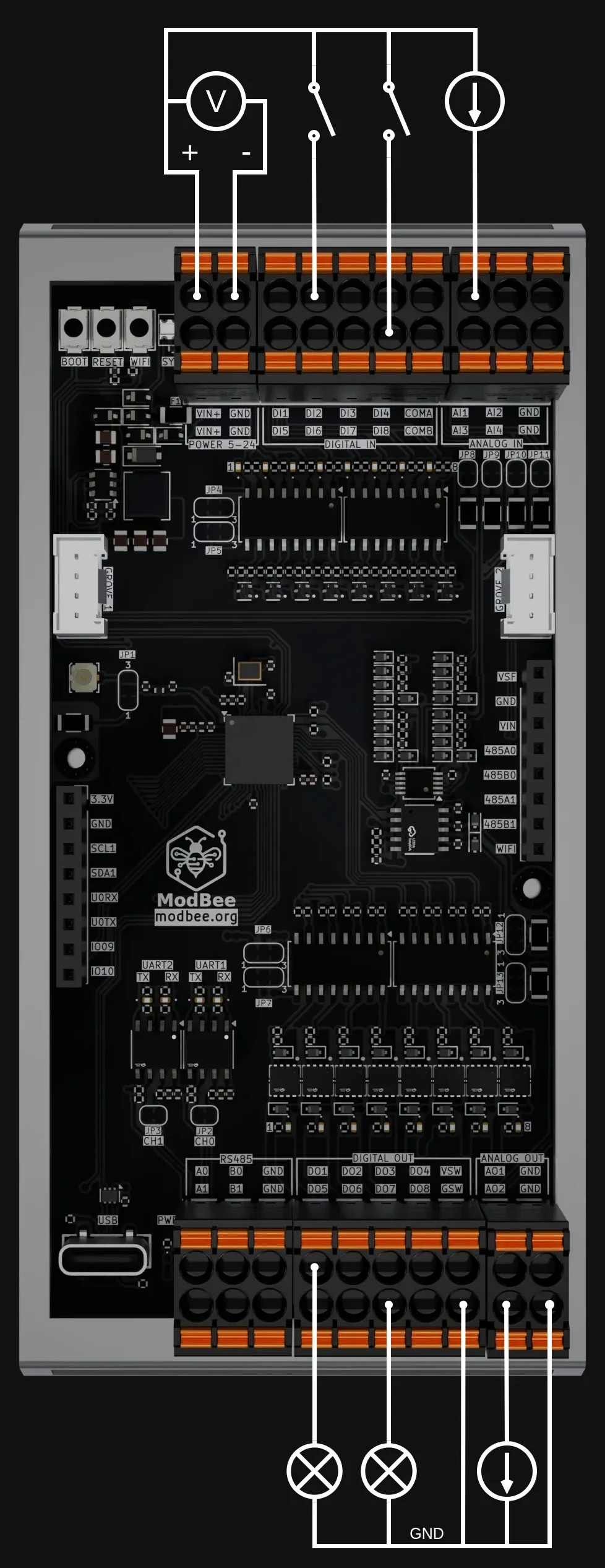
The Node-UIO is an I/O module built around the Espressif ESP32-S3FH4R2. It has:
- 8 opto-isolated digital inputs in two groups, each group with its own common
- 8 opto-isolated high-side (sourcing) MOSFET digital outputs
- 4 analog inputs on an ADS1115 16-bit ADC, 0-20 mA or 0-10 V per channel (solder bridge)
- 2 analog outputs on a GP8413 15-bit DAC, 0-10 V or 0-20 mA per channel (solder bridge)
- 2 RS485 ports
- 2.4 GHz Wi-Fi and Bluetooth LE (in the ESP32-S3)
- 2 Grove I2C connectors and two 8-pin stackable HAT headers
- An addressable RGB status LED and Reset, Boot and WiFi buttons
- USB-C (native USB of the ESP32-S3)
Specifications
| Item | Value |
|---|---|
| Microcontroller | ESP32-S3FH4R2, dual-core Xtensa LX7, up to 240 MHz |
| On-chip memory | 512 KB SRAM, 384 KB ROM, 16 KB RTC SRAM |
| In-package memory | 4 MB flash (quad SPI), 2 MB PSRAM (quad SPI) |
| Wireless | 2.4 GHz Wi-Fi (802.11 b/g/n), Bluetooth 5 (LE) |
| Antenna | Chip antenna (AE1) or U.FL connector (AE2), selected by JP1 |
| USB | USB-C (J1), ESP32-S3 native USB on GPIO 19/20, full speed |
| Supply input | 5-24 V DC on J2 (schematic note "5-24v Supply"), or USB VBUS (see Power) |
| Logic supply | 3.3 V from a synchronous buck regulator (U3) |
| Digital inputs | 8, opto-isolated, 5-24 V, two groups of four with separate commons |
| Digital outputs | 8, opto-isolated high-side MOSFET, 5-24 V; 100 mA max per output from the input supply, 500 mA max per output with a separate supply (schematic note, sheet 4) |
| Analog inputs | 4, ADS1115 at I2C address 0x49; 0-20 mA (as shipped) or 0-10 V per channel |
| Analog outputs | 2, GP8413 (15-bit) at I2C address 0x5F; 0-10 V (as shipped) or 0-20 mA per channel |
| Serial | 2 x RS485 (half duplex) |
| I2C | Internal bus GPIO 37/38 (ADC, DAC); external bus GPIO 47/48 (Grove, HAT) |
| Expansion | 2 x Grove (I2C, 3.3 V), HAT headers J6 and J7 (8 pins each) |
Part numbers not stated on the schematic: buck regulator U3, RS485
transceivers U2/U4, opto-couplers U5-U8, output MOSFETs Q11-Q18, input
transistors Q3-Q10, fuse F1, USB ESD device U10, and the protection diodes.
Their ratings are therefore not given here.
GPIO map
Every ESP32-S3 pin the board connects (sheet 1), and what the library does
with it.
| GPIO | Schematic net | Connected to | Library use |
|---|---|---|---|
| 0 | IO0 | Boot button SW2 (to GND). Strapping pin | Not used |
| 1-8 | DI_01-DI_08 | Digital input stages, sheet 3 | digitalIn() channels 0-7; deep-sleep wake source; pulse counting |
| 9 | GPIO9 | HAT header J6 pin 7 | HAT power enable, setHatPower() |
| 10 | GPIO10 | HAT header J6 pin 8 | Not used |
| 11-14 | DO_01-DO_04 | Digital output stages, sheet 4 | setDigitalOut() channels 0-3; can be held through deep sleep |
| 15 | U2TX | RS485 port 1 transceiver U4, DI | Not used |
| 16 | U2RX | RS485 port 1 transceiver U4, RO | Not used |
| 17 | U1TX | RS485 port 0 transceiver U2, DI | Not used |
| 18 | U1RX | RS485 port 0 transceiver U2, RO | Not used |
| 19 | D- | USB-C J1 via ESD device U10 | USB (CDC serial) |
| 20 | D+ | USB-C J1 via ESD device U10 | USB (CDC serial) |
| 21 | - | Not connected | - |
| 26-32 | - | In-package flash and PSRAM; not connected on the board | - |
| 33-36 | DO_05-DO_08 | Digital output stages, sheet 4 | setDigitalOut() channels 4-7; cannot be held through deep sleep |
| 37 | SDA_0 | ADS1115, GP8413; 4.7 kOhm pull-up (R4) | Converter bus Wire1, SDA |
| 38 | SCL_0 | ADS1115, GP8413; 4.7 kOhm pull-up (R5) | Converter bus Wire1, SCL |
| 39 | WS2812B | Status LED D10, data in | setLed() and the health indication |
| 40 | WIFI_EN | WiFi button SW3 (to 3.3 V), 10 kOhm pull-down R24; HAT header J7 pin 8 | button(), takeShortPress(), takeLongPress() |
| 41, 42 | - | Not connected | - |
| 43 | U0TX | HAT header J6 pin 6 | Not used |
| 44 | U0RX | HAT header J6 pin 5 | Not used |
| 45, 46 | - | Not connected. Strapping pins | - |
| 47 | SCL_1 | Grove J4/J5 pin 1, HAT J6 pin 3; 4.7 kOhm pull-up (R3) | Expansion bus Wire, SCL; i2cProbe(), expansionBus() |
| 48 | SDA_1 | Grove J4/J5 pin 2, HAT J6 pin 4; 4.7 kOhm pull-up (R2) | Expansion bus Wire, SDA; i2cProbe(), expansionBus() |
| CHIP_PU | RST | Reset button SW1, 10 kOhm pull-up R6, 1 uF C14 | - |
Notes:
- GPIO 3 is a strapping pin (JTAG signal source). It is only sampled if the
eFuse that enables that selection has been burned. On this board it is DI03. - GPIO 39-42 are the ESP32-S3 pin JTAG interface. GPIO 39 and 40 are used by
the LED and the WiFi button, so JTAG over pins is not available. JTAG over
USB (the USB Serial/JTAG controller) is unaffected. - Only GPIO 0-21 are RTC-capable on the ESP32-S3. That is why DO01-DO04
(GPIO 11-14) and the HAT enable (GPIO 9) can keep their level through deep
sleep and DO05-DO08 (GPIO 33-36) cannot. - The schematic's names for the RS485 UART nets (U1, U2) do not fix which UART
peripheral is used. The ESP32-S3 routes any UART to any of these pins.
Power
Sheet 2, "Synchronous Buck".
Input connector J2
| J2 pin | Signal |
|---|---|
| 1, 3 | V_IN (silkscreen VIN+) |
| 2, 4 | GND |
Supply rails
| Rail | Derived from | Feeds |
|---|---|---|
| V_IN | J2, or HAT header J7 pin 3 | Everything below |
| V_Supply | V_IN through diode D1, ahead of fuse F1 | Digital output supply V_Switch through JP6 (as shipped) |
| V_Supply_F | V_IN through fuse F1 and diode D2 | HAT header J7 pin 1 (silkscreen VSF); GP8413 DAC supply (VCC) |
| Buck input | V_IN through F1 and series diode D4, or USB VBUS through diode D6 | Buck regulator U3 |
| +3.3 V | U3 output | ESP32-S3, ADS1115, RS485 transceivers, status LED, input and output logic, Grove connectors, HAT J6 pin 1 |
- F1 is drawn as a resettable (PTC) fuse. Its rating is not stated.
- U3 output is set by the feedback divider R16 (100 kOhm) / R17 (22 kOhm).
U3's part number is not stated. - D8 with R19 (2.2 kOhm) is a power indicator LED on the 3.3 V rail.
- The "Voltage Supervisor" block (IC1, a MAX809 footprint, and C28) is marked
not fitted. Its note reads "Monitor 3.3v rail and switch off MCU
automatically or reset while being powered from 1s Batt".
Powering from USB only
USB VBUS reaches only the buck input. D4 stops it reaching V_IN, so on USB
power alone V_Supply and V_Supply_F are not powered (sheet 2). In that
condition:
- the GP8413 DAC has no supply, so the analog outputs do not work and
begin()reports the DAC missing (the status LED shows red); - the digital outputs have no supply as shipped (V_Switch comes from
V_Supply); - HAT J7 pin 1 (V_Supply_F) is not powered.
The ESP32-S3, the ADC, the RS485 ports, the digital input logic, the Grove
connectors and HAT J6 pin 1 (3.3 V) work from USB.
Supply voltage for the analog outputs
The GP8413 datasheet gives a supply range of 9-36 V (typical 12 V). Its VCC is
V_Supply_F, which is V_IN less the drop across F1 and D2. The analog outputs
therefore need V_IN of at least 9 V plus those drops. At the low end of the
board's 5-24 V input range they are outside the converter's specification.
Digital inputs
Sheet 3, "A Digital Inputs 1-4" and "B Digital Inputs 5-8".
Terminal J8
| Pin | Signal | Pin | Signal |
|---|---|---|---|
| 1 | DI01 | 6 | DI05 |
| 2 | DI02 | 7 | DI06 |
| 3 | DI03 | 8 | DI07 |
| 4 | DI04 | 9 | DI08 |
| 5 | COM A (DI01-DI04) | 10 | COM B (DI05-DI08) |
Circuit
Each input feeds the LED of an opto-coupler (U5, U6) through 5.1 kOhm. A
second branch, 10 kOhm and an indicator LED (D11-D18), lights when the input
is on. The opto-coupler output drives a PNP transistor (Q3-Q10) whose
collector, with a 47 kOhm pull-down, is the GPIO.
- Rated input: 5-24 V DC (sheet 3 note).
- Polarity: current flows into the DI terminal and out through the group's
return. The DI terminal must be positive with respect to that return. - Logic: an energised input reads high at the GPIO.
digitalIn()returns
truefor an energised input. - Group return: the opto LED returns of each group go to the centre pad of a
three-pad solder jumper (JP4 for DI01-DI04, JP5 for DI05-DI08). Pad 1 is
board GND and pad 3 is the group's COM terminal. The sheet note reads "Cut
bridge 1&2 to use isolated supply". As shipped (pads 1-2 bridged), the inputs
return to board GND and are not isolated from it. See
Solder bridges.
Library features
- Wake from sleep:
sleep()takes a mask of inputs that wake the board on a
high level (ESP32-S3 ext1 wake). - Pulse counting:
pulseStart(),pulseCount()andpulseStop()count
rising edges on any input with the ESP32-S3 pulse counter (PCNT). The chip
has four counter units, so four inputs can be counted at once. The maximum
pulse rate the input circuit passes is not specified.
Digital outputs
Sheet 4, "A Digital Outputs 1-4" and "B Digital Outputs 5-8".
Terminal J9
| Pin | Signal | Pin | Signal |
|---|---|---|---|
| 1 | DO01 | 6 | DO05 |
| 2 | DO02 | 7 | DO06 |
| 3 | DO03 | 8 | DO07 |
| 4 | DO04 | 9 | DO08 |
| 5 | VSW (JP6 pad 3) | 10 | GSW (JP7 pad 3) |
Circuit
The GPIO drives the LED of an opto-coupler (U7, U8) through 470 Ohm, with a
47 kOhm pull-down. Each output MOSFET (Q11-Q18) is a high-side switch between
V_Switch and the DO terminal. Its gate is held to V_Switch by 10 kOhm and a
clamp diode, and the opto-coupler pulls it toward G_Switch through 1 kOhm to
turn the output on. When the output is on, the DO terminal is connected to
V_Switch.
- The outputs source current. Connect the load between the DO terminal and the
supply return (GND, or GSW on J9 pin 10). - Each output has an indicator LED (D23-D26, D35-D38) and a diode from the
output to G_Switch (D27-D30, D39-D42). - All eight outputs share one V_Switch and one G_Switch. The "A" and "B"
groups are separate drawings, not separate supplies. - Ratings (sheet 4 note): "5-24v Outputs switched from Input Supply by default
100ma MAX per output. If jumpers cut or separate supply wire used in
terminal 5 500ma MAX per output." - Supply selection: JP6 (pad 1 V_Supply, pad 2 V_Switch, pad 3 J9 pin 5) and
JP7 (pad 1 GND, pad 2 G_Switch, pad 3 J9 pin 10). The sheet note reads "Cut
Bridge 1&2 to use an Isolated separate supply and Ground". See
Solder bridges.
Library behaviour
begin()drives every output low before anything else.setDigitalOut()sets an output anddigitalOut()reads the commanded
state back. The pins are written on eachupdate().- In deep sleep, DO01-DO04 can be held at a chosen level (the
outputsInSleepargument ofsleep()). DO05-DO08 are outside the RTC domain
and turn off.
Analog inputs
Sheet 5, "0-20ma/0-10v Analog Inputs" and "ADS1115 16bit ADC".
Terminal J10
| Pin | Signal | Pin | Signal |
|---|---|---|---|
| 1 | AI01 | 4 | AI03 |
| 2 | AI02 | 5 | AI04 |
| 3 | GND | 6 | GND |
Circuit
Per channel: a shunt resistor (R100-R103) to GND through a solder bridge
(JP8-JP11), then 1 kOhm in series, clamp diodes, and a 47 kOhm / 12 kOhm divider
to the ADC input, with clamp diodes to 3.3 V and GND and 100 nF to GND.
- As shipped, the bridge is closed and the channel measures 0-20 mA (sheet 5
note: "0-20ma Default Cut Bridge to use 0-10v"). - Cut the channel's bridge for 0-10 V.
- The shunt resistor values are not stated on the schematic.
- In 0-10 V mode the terminal sees 60 kOhm to GND (1 + 47 + 12 kOhm), and the
ADC pin sees 12/60 of the terminal voltage. With the converter at
+/-2.048 V, its full count therefore corresponds to 10.24 V at the terminal,
so an uncalibrated 0-10 V reading is about 2.3 % low. Calibrate each channel
(see below).
| Channel | ADS1115 input | Bridge | Shunt |
|---|---|---|---|
| AI01 | AIN0 | JP8 | R100 |
| AI02 | AIN1 | JP9 | R101 |
| AI03 | AIN2 | JP10 | R102 |
| AI04 | AIN3 | JP11 | R103 |
Converter
- ADS1115IDGS (U9), supplied from 3.3 V.
- I2C address 0x49: ADDR is tied to VDD (sheet 5 note "Default I2c Address
0x49"; ADS1115 datasheet, ADDR pin table). - On the internal bus, GPIO 37 (SDA) / GPIO 38 (SCL).
- ALERT/RDY is pulled up through 10 kOhm and not connected to the MCU.
- The library sets the full-scale range to +/-2.048 V (the sheet 5 note asks
for this), single-shot mode, 250 samples per second, and converts the four
channels in turn.
Range in software
The solder bridge sets what a terminal accepts. setInputRange() only sets
the scaling, and it defaults to UIO_VOLTAGE on every channel. A channel left
in the factory 0-20 mA configuration must be set to UIO_CURRENT by the
program, or its reading is wrong.
Uncalibrated, the library maps the converter's full count (32767) to 10 V or
20 mA. Use setInputCalibration(), saveCalibration() and
resetCalibration() for two-point calibration, which is stored in NVS.
analogInRaw() returns the converter count.
Analog outputs
Sheet 5, "0-20ma/0-10v Analog Outputs".
Terminal J11
| Pin | Signal |
|---|---|
| 1 | AO01 |
| 2 | GND |
| 3 | AO02 |
| 4 | GND |
Circuit
- GP8413 (IC2), dual-channel 15-bit voltage-output DAC. VOUT0 is AO01 and
VOUT1 is AO02. - Supply VCC from V_Supply_F. The datasheet range is 9-36 V; see
Power. - I2C address 0x5F: A0, A1 and A2 are tied to 3.3 V (sheet 5 note "Default
I2c Address 0x5F"). The GP8413 address is 0x58 plus A2-A0. - On the internal bus, GPIO 37 (SDA) / GPIO 38 (SCL).
- Each output has 100 nF and a clamp diode (D63, D64) to GND.
- Range: a three-pad solder bridge per channel (JP12 for AO01, JP13 for AO02).
Pad 1 is the DAC output, pad 3 is the DAC output through a series resistor
(R120, R121), and pad 2 is the terminal. As shipped, pads 1-2 are bridged
and the output is 0-10 V. The sheet note reads "0-10v Default Cut Bridge 1&2
to use 0-20ma". The terminal then connects only through pad 3, so pads 2-3
must be bridged. R120 and R121 values are not stated on the schematic. - In 0-20 mA mode the output is the DAC voltage through the series resistor.
The GP8413 is a voltage-output converter, so the current also depends on
the load resistance. Calibrate against the actual load. - The GP8413 datasheet does not state an output current rating.
Library behaviour
begin()sets the GP8413 to its 0-10 V range.setAnalogOut()takes volts or milliamps according tosetOutputRange(),
which defaults toUIO_VOLTAGE. That matches the factory bridge.- Uncalibrated, 10 V or 20 mA maps to the full count (32767).
setOutputCalibration()adjusts this.analogOutRaw()returns the count
written. - The DAC is written only when a value changes.
RS485
Sheet 2, "RS485 Transceiver CH1" (port 0) and "RS485 Transceiver CH2"
(port 1). The board provides the transceivers only. This library does not open
the ports. Modbus RTU or ModBee protocol libraries can run over them.
Terminal J3
| Pin | Signal | Pin | Signal |
|---|---|---|---|
| 1 | A0 (RS485_A_0) | 4 | A1 (RS485_A_1) |
| 2 | B0 (RS485_B_0) | 5 | B1 (RS485_B_1) |
| 3 | GND | 6 | GND |
The A and B lines of both ports are also on HAT header J7.
Per port
| Port 0 | Port 1 | |
|---|---|---|
| Transceiver | U2 | U4 |
| TX (MCU to DI) | GPIO 17 (U1TX) | GPIO 15 (U2TX) |
| RX (RO to MCU) | GPIO 18 (U1RX) | GPIO 16 (U2RX) |
| Termination | R18, 120 Ohm, via JP2 | R27, 120 Ohm, via JP3 |
| Bias | A: 1 kOhm to 3.3 V (R14); B: 1 kOhm to GND (R15) | A: R25; B: R26 (same values) |
| Activity LEDs | D66 (TX), D65 (RX) | D68 (TX), D67 (RX) |
- Direction: DE and RE of each transceiver are tied to 3.3 V on the
schematic. No GPIO controls direction. The transceiver part number is not
stated; see the schematic. - RO and DI each have a 10 kOhm pull-up to 3.3 V.
- Termination: the sheet note reads "Cut Bridge to disable 120ohm EOL
termination resistor". Fit termination only at the two ends of a bus. - Pins: the Arduino-ESP32 core's default pins for
Serial1andSerial2on
the ESP32-S3 are not these. Pass the RX and TX pins above when opening a
port.
Expansion
HAT headers J6 and J7
Sheet 2, "Stackable Header Pins for Hats".
| J6 pin | Signal | J7 pin | Signal |
|---|---|---|---|
| 1 | +3.3 V | 1 | V_Supply_F (silkscreen VSF) |
| 2 | GND | 2 | GND |
| 3 | SCL_1 (GPIO 47) | 3 | V_IN |
| 4 | SDA_1 (GPIO 48) | 4 | RS485_A_0 |
| 5 | U0RX (GPIO 44) | 5 | RS485_B_0 |
| 6 | U0TX (GPIO 43) | 6 | RS485_A_1 |
| 7 | GPIO 9 | 7 | RS485_B_1 |
| 8 | GPIO 10 | 8 | WIFI_EN (GPIO 40, WiFi button) |
Sheet 2 note: "V_Supply_F Fused Supply to Hat. V_IN Supply AUX power From
Hat". The note also advises a diode on the HAT if needed. J7 pin 3 connects
directly to V_IN, ahead of the fuse. A HAT can supply the board through it.
HAT power enable: the base board connects GPIO 9 to J6 pin 7 and nothing
else. It has no switch of its own on this line, so any switching is done on
the HAT. The library drives GPIO 9 with setHatPower() (low after begin())
and reports it with hatPower(). sleep() can hold it through deep sleep
(hatInSleep).
Grove connectors J4 and J5
Sheet 2, note "Grove Connectors I2C 3.3V MAX". Both connectors are identical:
| Pin | Signal |
|---|---|
| 1 | SCL_1 (GPIO 47) |
| 2 | SDA_1 (GPIO 48) |
| 3 | +3.3 V |
| 4 | GND |
Use 3.3 V I2C devices only. The bus has 4.7 kOhm pull-ups to 3.3 V (R2, R3).
Two I2C buses
The schematic has two separate I2C buses:
| Bus | Pins | Connected to |
|---|---|---|
| SDA_0 / SCL_0 | GPIO 37 / 38 | ADS1115 (0x49), GP8413 (0x5F) only |
| SDA_1 / SCL_1 | GPIO 48 / 47 | Grove J4, J5 and HAT J6 |
begin() starts both: Wire1 for the converters and Wire for the
expansion bus. The library's expansion functions (i2cProbe(),
expansionBus()) use Wire, so they reach what is plugged into the Grove
connectors and the HAT header. The converters have their bus to themselves,
so any address is free on the expansion bus, including 0x49 and 0x5F.
Buttons and LEDs
| Item | Designator | Connection | Notes |
|---|---|---|---|
| Reset | SW1 | CHIP_PU to GND; 10 kOhm pull-up, 1 uF | Resets the ESP32-S3 |
| Boot | SW2 | GPIO 0 to GND | Hold during reset for download mode |
| WiFi | SW3 | GPIO 40 to 3.3 V; 10 kOhm pull-down (R24); also HAT J7 pin 8 | Active high |
| Status LED | D10 | Addressable RGB LED (net WS2812B), data on GPIO 39, supplied from 3.3 V | Sheet 2 legend: green = MCU OK, red = fault, blue = status |
| Power LED | D8 | 3.3 V rail through 2.2 kOhm | |
| Input LEDs | D11-D18 | Field side of each digital input | |
| Output LEDs | D23-D26, D35-D38 | Each digital output | |
| RS485 LEDs | D65-D68 | TX and RX lines of each port |
WiFi button: the sheet 2 note gives the intended use, "Short Press Enable WIFI
for set time. Long Press Reset EEPROM Press > 30sec". The library does not
implement either action. It reports presses: button(), buttonHeldMs(),
takeShortPress() and takeLongPress(). A long press defaults to 2000 ms
(setButtonLongMs()), with 30 ms debounce (setButtonDebounceMs()).
setRadioPolicy() and requestRadio() are the library's radio duty-cycle
controls, which a program can tie to the button.
Status LED: until setLed() is called, the library shows green when both the
ADS1115 and the GP8413 answered at begin() and red when either did not.
setLed() takes the LED over. sleep() can leave it at a dim blue
(ledInSleep).
Solder-bridge configuration
All configuration is by solder jumper. There is no software control of any of
these. "As shipped" is taken from the sheet notes. Check the board before you
rely on it, especially for JP1, which has no note.
| Designator | Sheet | Pads | As shipped | Change |
|---|---|---|---|---|
| JP1 | 1 | 2 = RF feed; 1 = chip antenna AE1; 3 = U.FL AE2 | Not stated on the schematic | Bridge 2-1 for the chip antenna or 2-3 for U.FL |
| JP2 | 2 | 120 Ohm termination R18, port 0 | Bridged (termination on) | Cut to remove termination |
| JP3 | 2 | 120 Ohm termination R27, port 1 | Bridged (termination on) | Cut to remove termination |
| JP4 | 3 | 1 = GND, 2 = DI01-DI04 return, 3 = COM A (J8 pin 5) | 1-2 bridged: return to board GND | Cut 1-2 to use an isolated supply on COM A |
| JP5 | 3 | 1 = GND, 2 = DI05-DI08 return, 3 = COM B (J8 pin 10) | 1-2 bridged: return to board GND | Cut 1-2 to use an isolated supply on COM B |
| JP6 | 4 | 1 = V_Supply, 2 = V_Switch, 3 = VSW (J9 pin 5) | 1-2 bridged: outputs switch V_Supply | Cut 1-2 to use a separate supply on VSW |
| JP7 | 4 | 1 = GND, 2 = G_Switch, 3 = GSW (J9 pin 10) | 1-2 bridged: G_Switch is board GND | Cut 1-2 to use a separate ground on GSW |
| JP8-JP11 | 5 | Shunt R100-R103 to GND, AI01-AI04 | Bridged: 0-20 mA | Cut for 0-10 V |
| JP12, JP13 | 5 | 1 = DAC direct, 2 = terminal, 3 = via R120/R121; AO01, AO02 | 1-2 bridged: 0-10 V | Cut 1-2 and bridge 2-3 for 0-20 mA |
The state of pads 2-3 on JP4-JP7, as shipped, is not shown on the schematic.
Not fitted (marked DNP on the schematic): IC1 (MAX809 supervisor) and C28 on
sheet 2; C17, C18 and R9 (antenna matching) on sheet 1.
Programming
- Connector: USB-C J1, wired to the ESP32-S3 native USB pins (GPIO 19/20).
CC1 and CC2 have 5.1 kOhm pull-downs (R7, R8). There is no USB-to-UART
bridge. - Serial: the example build (
platformio.ini) setsARDUINO_USB_MODE=1and
ARDUINO_USB_CDC_ON_BOOT=1, soSerialis USB CDC on the native port. UART0
(GPIO 43/44) goes only to HAT header J6. - Download mode: hold BOOT (SW2), press and release RESET (SW1), then release
BOOT. With GPIO 0 low at reset and GPIO 46 low (not connected; internal
pull-down), the ESP32-S3 enters joint download boot, which includes USB
download. - Debug: JTAG is available over USB (USB Serial/JTAG controller). It is not
available over pins, because GPIO 39 and 40 are used on the board.
For the software interface, see API.md.