
Hardware
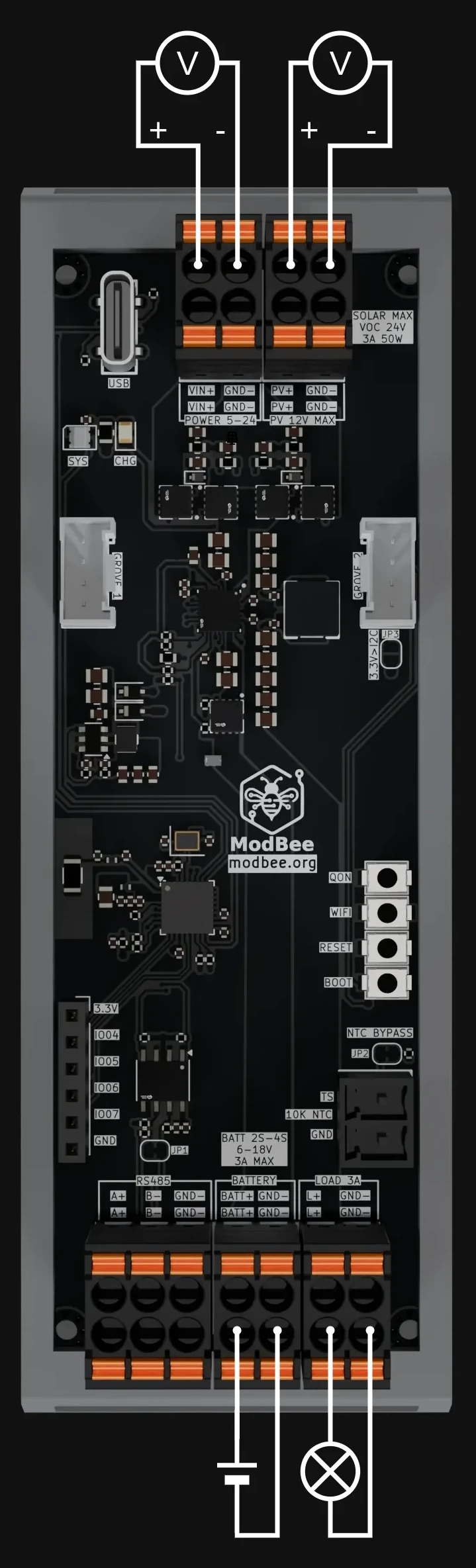
Hardware reference for the ModBee MPPT Charger (ESP32-C3 + TI BQ25798). Everything here is taken from the schematics in schematics/ and the board silkscreen. Chip specifications refer to the TI BQ25798 datasheet (SLUSDV2) and the Espressif ESP32-C3 datasheet.
Contents
- Board ratings
- Connectors
- Connection and disconnection order
- Block diagram
- BQ25798 charger
- Inputs and protection
- 3.3 V rail and USB-C
- ESP32-C3 and pin map
- RS485
- Grove I2C
- Battery temperature (NTC)
- LEDs, buttons and jumpers
- Schematic revisions
- Battery voltage reference
Board ratings
These are the limits printed on the board. Stay inside them.
| Item | Rating |
|---|---|
| POWER input (VIN) | 5 V to 24 V DC |
| PV input | 12 V nominal panel; Voc 24 V max, 3 A, 50 W |
| Battery | 2S to 4S lithium, 6 V to 18 V, 3 A max |
| Load output | 3 A |
| Grove I2C | 3.3 V logic only |
| Mounting | 35 mm DIN rail enclosure, 118 × 42 × 45 mm (L × W × H) |
Notes:
- PV Voc limit. The BQ25798 operates from 3.6 V to 24 V and has a 30 V absolute maximum. TI states that panel Voc must not exceed 24 V. Panel Voc rises in cold weather, so size the panel from its cold-temperature Voc. A "12 V" (36-cell) panel fits; a "24 V" panel (Voc 36 V to 45 V) will destroy the charger.
- Battery range. The BQ25798 itself supports 1S to 4S. The board is rated for 2S to 4S because the 3.3 V buck runs from the SYS rail, which follows the battery voltage.
- There is no reverse-polarity protection on the power terminals. Check polarity before connecting anything.
- Inputs. A reversed supply goes straight to the BQ25798 VAC1/VAC2 sense pins, which are rated to -2 V. The input FET pairs block reverse current from VBUS back out of an input; they do not protect against reversed polarity.
- Battery. A reversed battery reverse-biases the polarised bulk capacitors on BAT+ (C53, C55).
Connectors
All power and RS485 terminals are 2-position push-in terminals, doubled (two contacts per signal).
| Silkscreen | Schematic | Net | Function |
|---|---|---|---|
| POWER 5-24 (VIN+, GND-) | J2 | VDC_IN → VAC1 | DC adapter / second supply input |
| PV (PV+, GND-) | J3 | PV_IN → VAC2 | Solar panel input |
| BATTERY (BATT+, GND-) | J5 | BAT+ | Battery |
| LOAD 3A (L+, GND-) | J4 | VDC_SYS | Load output (BQ25798 SYS rail) |
| RS485 (A+, B-, GND-) | J6 | RS485_A / RS485_B | RS485 bus |
| GROVE 1, GROVE 2 | J7, J8 | SCL_0 / SDA_0 / 3.3V_I2C / GND | Hardware I2C expansion |
| TS / 10K NTC / GND | J11 | TS_1 | Battery NTC thermistor |
| 3.3V, IO04-IO07, GND | J10 | GPIO4-GPIO7 | Spare GPIO / debug header |
| USB | J1 | VUSB, D+/D- | Programming, serial console, logic power |
Connect loads to LOAD, not directly to the battery. The LOAD terminal is the BQ25798 SYS rail. It is supplied from the inputs when they are present, falls back to the battery when they are not, and the charger accounts for its current.
Connection and disconnection order
The BQ25798 CE pin is tied to GND, so charging is enabled in hardware by design. This lets the board run unattended: it starts charging on its own after any power interruption. The charge voltage and current, however, come from the settings saved in the firmware. Until the ESP32-C3 has applied them, the charger runs on its power-on defaults. With the fitted 18 kΩ PROG resistor these defaults are 4S, 16.8 V, 1 A (see BQ25798 charger).
The order below makes sure the firmware has applied the saved settings before any charging source is present.
Connecting
- Battery first. Connect BATT+ and GND-. The BQ25798 and the ESP32-C3 power up from the battery (no charging is possible yet), and the firmware writes the saved battery settings to the charger.
- Expect a small spark: rev 0.02 has 2 × 100 µF of bulk capacitance on BAT+.
- Fit a fuse close to the battery.
- Wait for the status LED to come on before continuing.
- PV and/or POWER input second. Charging starts using the settings already applied.
- Load last. Connect the load once the board is running normally.
Disconnecting
- Load first. This avoids breaking load current at the terminals and stops the load from draining the battery while you work.
- PV and/or POWER input second. Charging stops and the board runs from the battery.
- Battery last. The board powers down.
Avoid
- Connecting PV or POWER with no battery, then adding the battery. The BAT terminal is already live and regulating toward the charger's current target voltage. If the firmware has not applied the saved settings (no battery settings yet, failed boot, corrupt filesystem), that target is the 4S PROG default.
- Removing the battery while an input is connected. The board drops to input-only operation, which is unstable on solar.
- Hot-plugging a 4S pack on long leads without the BAT TVS. TI recommends a TVS for this case; it is fitted from rev 0.02 (D7).
Block diagram
 POWER (VAC1) ──► Q1/Q3 ─┐
                         ├─► VBUS ──► BQ25798 buck-boost ──► SYS ──┬──► LOAD terminal
 PV    (VAC2) ──► Q2/Q4 ─┘            (MPPT, I2C)                  │
                                          │                        └──► D1 ─┐
                                          ▼                                 ├──► 3.3 V buck ──► ESP32-C3,
                                   BAT ──► Q5 (ship FET) ──► BATTERY  USB ─► D2 ─┘   RS485, LED, Grove (JP3)
BQ25798 charger
| Item | Value |
|---|---|
| I2C | 7-bit address 0x6B, on the ESP32-C3 software I2C bus (GPIO2 = SCL, GPIO3 = SDA, 4.7 kΩ pull-ups) |
| Inductor | 1.0 µH (L4) |
| PROG resistor | 18 kΩ (R21) |
| CE_N | Tied to GND: charging enabled in hardware |
| ILIM_HIZ | Tied to REGN through 0 Ω (R20): no hardware input current clamp |
| QON_N | QON button (SW4) to GND |
| INT_N | GPIO1, 10 kΩ pull-up to 3.3 V |
| STAT | Green CHG LED (D6) |
| D+/D- | Not connected (no USB adapter detection) |
| Ship FET | External N-FET Q5 on SDRV |
PROG resistor and power-on defaults. The PROG pin sets the cell count and switching frequency at power-on (datasheet Table 7-1). The fitted 18 kΩ selects 4S at 1.5 MHz (TI's nominal value for this setting is 17.4 kΩ). The resulting power-on defaults are:
- VREG 16.8 V
- ICHG 1 A
- VSYSMIN 12 V
These are the hardware fallback. The firmware overrides them with the saved settings at boot and re-applies them periodically.
Charger features used:
- Buck-boost charging. 1S to 4S, VREG 3.0 V to 18.8 V in 10 mV steps, ICHG 50 mA to 5 A in 10 mA steps. The board is rated 3 A.
- MPPT. The BQ25798 periodically stops switching to sample the panel's open-circuit voltage (VOC). It then sets the input voltage regulation point (VINDPM) to a selectable fraction of VOC: 56.25 % to 100 %, firmware default 87.5 %.
- NVDC power path. SYS follows the battery voltage, with a floor at VSYSMIN.
- Integrated ADC. Measures input, battery and system voltage and current, plus the TS and die temperature.
- Protection (from the datasheet):
- VBUS OVP at 26 V typ
- VAC OVP selectable at 7, 12, 18 or 26 V
- Battery OVP at 104 % of VREG
- Thermal regulation (default 120 °C) and shutdown (default 150 °C)
- Charge safety timer (5, 8, 12 or 24 h)
- JEITA battery temperature control via TS
Inputs and protection
Each input has a back-to-back N-FET pair driven by the BQ25798 ACDRV outputs (VAC1: Q1/Q3, VAC2: Q2/Q4). Each pair has a 12 V gate-source Zener (D4/D5) and a 270 Ω gate resistor.
- Input selection. The BQ25798 selects one input at a time. When both are present at power-up, VAC1 (POWER) is the primary input (datasheet §7.3.5). When the selected input is removed, the charger switches to the other input if it is valid.
- Reverse blocking. The FET pair blocks reverse current from VBUS back into an unused input.
Protection on the power path (rev 0.02):
| Location | Parts | Purpose |
|---|---|---|
| VDC_IN, PV_IN | D8, D9 TVS | Input transient clamp (new in rev 0.02) |
| VDC_IN, PV_IN | R17/C27, R18/C28 (2 Ω + 1 µF) | Hot-plug RC snubber, as recommended by TI for inputs above 15 V |
| BAT+ | D7 bidirectional TVS | Battery hot-plug clamp (unidirectional in rev 0.01) |
| BAT+ | C53, C55 (2 × 100 µF) | Bulk capacitance (new in rev 0.02) |
| BAT (charger side) | R30 + C41 (2 Ω + 10 µF) | RC damping (new in rev 0.02) |
| SYS / LOAD | D10 TVS, C54 (100 µF) | Load-side clamp and bulk capacitance (new in rev 0.02) |
3.3 V rail and USB-C
- 3.3 V buck (U1). A synchronous buck converter with a 6.8 µH inductor and a 100 kΩ / 22 kΩ feedback divider. It is fed from SYS (through D1) or from USB VBUS (through D2), whichever is higher. It supplies the ESP32-C3, RS485 transceiver, status LED and, through JP3, the Grove ports.
- USB-C (J1). Wired to the ESP32-C3 native USB Serial/JTAG (GPIO18/GPIO19), with 5.1 kΩ CC pull-downs (5 V sink).
- USB powers the 3.3 V logic only. It does not feed the charger and cannot charge the battery.
- With only USB connected, the BQ25798 is unpowered and does not respond on I2C.
ESP32-C3 and pin map
The MCU is an ESP32-C3FH4 chip: single-core RISC-V up to 160 MHz, 400 KB SRAM, 4 MB in-package flash, 2.4 GHz Wi-Fi 4 (802.11 b/g/n) and Bluetooth 5 LE. It uses a 40 MHz crystal and an on-board chip antenna (AE1) with a matching network. There is no external antenna connector.
| GPIO | Net | Function | Used by firmware |
|---|---|---|---|
| GPIO0 | WIFI_EN | WIFI button (SW3), active high, 10 kΩ pull-down | Yes |
| GPIO1 | INT_N | BQ25798 interrupt (open drain, 10 kΩ pull-up) | Not yet |
| GPIO2 | SCL_1 | Software I2C clock to BQ25798 | Yes |
| GPIO3 | SDA_1 | Software I2C data to BQ25798 | Yes |
| GPIO4-GPIO7 | IO04-IO07 | J10 header | No |
| GPIO8 | SDA_0 | Hardware I2C data, Grove ports | Not yet |
| GPIO9 | SCL_0 | Hardware I2C clock, Grove ports; BOOT button (SW2) | Not yet |
| GPIO10 | WS2812B | RGB status LED data | Yes |
| GPIO18/GPIO19 | D-/D+ | USB-C | Yes (programming, serial console) |
| GPIO20 | U0RXD | RS485 receiver output (RO) | Not yet |
| GPIO21 | U0TXD | RS485 driver input (DI) | Not yet |
| CHIP_EN | CHIP_EN | RESET button (SW1), 10 kΩ / 1 µF RC | Yes |
The ESP32-C3 has one hardware I2C controller. It is kept free for the Grove ports, so the BQ25798 is on a software I2C bus.
RS485
- Transceiver. U2 is an automatic-direction RS485 transceiver connected to UART0 (GPIO20 = RO, GPIO21 = DI), with 10 kΩ pull-ups on RO and DI. RE and DE are tied to 3.3 V; no GPIO is used for direction control.
- Failsafe bias. A 1 kΩ pull-up on A and a 1 kΩ pull-down on B.
- Termination. A 120 Ω resistor (R15) is connected by solder bridge JP1. Cut JP1 to remove it on nodes that are not at either end of the bus.
- Connector. J6: A+, B-, GND-.
The firmware does not yet implement Modbus or any other RS485 protocol (see the README).
Grove I2C
There are two Grove connectors (GROVE 1, GROVE 2) on the hardware I2C bus (GPIO8 = SDA, GPIO9 = SCL), with 4.7 kΩ pull-ups to 3.3 V. 3.3 V logic only.
The Grove VCC pin (3.3V_I2C) is not connected by default. Bridge JP3 ("3.3V>I2C") only when the board should power the attached sensor. Leave it open if the Grove bus is powered by another board, so two supplies are never tied together.
Battery temperature (NTC)
- Thermistor. Connect a 10 kΩ NTC (103AT type) to the TS terminal (J11).
- Bias network. TS is biased from REGN by R27 (5.1 kΩ) and R28 (30 kΩ), close to TI's reference values (5.24 kΩ / 30.31 kΩ). The BQ25798 then applies its JEITA temperature window: by default it suspends charging below 0 °C and above 60 °C, and reduces charge current or voltage between those limits.
- No thermistor. Bridge JP2 ("NTC BYPASS") to fit a fixed 10 kΩ (R29) in place of the thermistor. Otherwise TS sits outside the VT1-VT5 window and the BQ25798 suspends charging.
LEDs, buttons and jumpers
| Item | Silkscreen | Function |
|---|---|---|
| D3 WS2812B RGB LED | SYS | Firmware status (see below) |
| D6 green LED | CHG | BQ25798 STAT: on while charging, off when charge is done or disabled, blinks at 1 Hz on a charger fault |
| SW3 | WIFI | Short press: turn on the Wi-Fi access point |
| SW1 | RESET | Resets the ESP32-C3 (CHIP_EN) |
| SW2 | BOOT | Hold while pressing RESET to enter the ROM bootloader |
| SW4 | QON | BQ25798 QON: wakes the charger from ship mode |
| JP1 | (RS485 area) | 120 Ω RS485 termination, closed by default; cut to disable |
| JP2 | NTC BYPASS | Fixed 10 kΩ in place of the battery NTC |
| JP3 | 3.3V>I2C | Connect 3.3 V to the Grove VCC pins |
SYS LED colours set by the firmware:
| Colour | Meaning |
|---|---|
| Orange | Starting up |
| Red | Charger fault reported by the BQ25798 |
| Yellow | Charging |
| Green | Charge complete |
| Blue | Idle (not charging) |
Schematic revisions
| File | Revision | Date |
|---|---|---|
| modbee-mppt-ti-c3.pdf | 0.01 | 2025-05-16 |
| modbee-mppt-ti-c3-rev0.02.pdf | 0.02 | 2026-04-13 |
Rev 0.02 changes the charger sheet only. It adds:
- TVS diodes on both inputs (D8, D9) and on SYS (D10); D7 on BAT+ becomes bidirectional.
- 100 µF bulk capacitors on BAT+ (C53, C55) and SYS (C54).
- An RC damper (R30, C41) on the charger BAT node, and an extra 10 µF on BAT (C56).
The MCU and connector sheets are unchanged.
Battery voltage reference
Use the manufacturer's datasheet for your cells. Typical values:
| Chemistry | Nominal / cell | Charge voltage / cell | 2S | 3S | 4S |
|---|---|---|---|---|---|
| Li-ion / Li-Po | 3.6-3.7 V | 4.20 V | 8.4 V | 12.6 V | 16.8 V |
| LiFePO4 | 3.2 V | 3.60-3.65 V | 7.2-7.3 V | 10.8-10.95 V | 14.4-14.6 V |
The BQ25798 is specified by TI for Li-ion and Li-polymer. LiFePO4 is supported by setting the charge voltage, as above. Lead-acid is not a suitable chemistry for this charger: it has no float stage and its cell voltages do not map onto the BQ25798 cell-count windows.